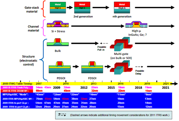
Pursuit of high performance computation is endless desire of human being. This desire has given birth to Silicon Valley previously mentioned, modern society and this article. Moors’ Law serves so well in scaling down of transistor and Dennard’s Scaling Theory as more technical guide until very recent. It is very interesting to look into how the skyscraper of computation built up from single transistor to integrated circuit to hardware system such as personal computer, big server, even supercomputer. It is a bottom-up process in which lower level gives solid support to higher level. As maturity of semiconductor industries, society focus shift upwards to levels where holds more innovation and chaos, namely, software and cloud computing. But semiconductor is still a trunk which feeds a whole bunch of branches. How to keep it evergreen? Here are the plans intrigued by Brian’s presentation.
Plan A: Transistor Scaling
Scaling is predicted down to 8 nm. Currently Intel reaches to 22 nm by introduction of tri-gate structure. 3D integration is kind of another way to scale. Stacking of heterogenous IC could give more functions and lower power consumptions per area.

IDF 2011
Plan B: Circuit and System Design
If the physical limit are approaching, here is the near term issue we can look into. Innovations are demanded to optimize IC performance, power and variability. Non-volatile memory and multi-core computation are promising.

Plan C: Exploratory Research
Exotic material such as nanotube, graphene and quantum dot, new device like spintronics, also quantum computation.

A magnetologic gate, which consists of graphene contacted by several magnetic electrodes.
Reference:
THE INTERNATIONAL TECHNOLOGY ROADMAP FOR SEMICONDUCTORS: 2010 UPDATE


