Raman spectroscopy in graphene and nanoribbons

Abstract

Raman spectroscopy in bulk graphene and nanoribbons are reviewed. First, a short introduction of graphene crystal structure and phonon dispersion is given. First-order and the double resonance Raman scattering mechanism in graphene are discussed to understand the most prominent Raman peaks. Raman in bulk graphene is discussed for numbers of layers with different stacking and substrate effects. Finally, we try to distinguish the zigzag and armchair type of graphene edges and the differences of Raman signal in nanoribbon and bulk graphene are discussed.

  • Introduction

Graphene is a remarkable, two-dimensional material that has a number of unique electronic properties arising from a combination of its zero-gap linear dispersion, high carrier mobility, and high thermal conductivity. These electronic properties make graphene a leading contender to replace Si-based or III-V materials-based devices for high-frequency FET,1 post-CMOS nanoelectronic devices,2,3 and for use in even more futuristic devices based on photonics,4 spintronics5,6 and quantum computing.7 Graphene’s combination of low mass and high mean free path leads to very high electronic mobility, with a record value of 230,000 cm2/V-sec for suspended graphene sheets.8

Crystal structure of graphene

Graphene is a two-dimensional (2D) planar structure based on a unit cell containing two carbon atoms A and B, as shown in Fig. 1. The structure can be seen as a triangular lattice composed by two vectors a1, a2 with a basis of two atoms per unit cell.


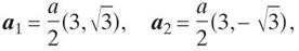
Where is the lattice constant of monolayer graphene. Likewise, the unit cell in reciprocal space is shown in Fig. 1 and is described by the unit vectors b1 and b2 of the reciprocal lattice given by

corresponding to a lattice of length in reciprocal space. The unit vectors b1 and b2 of the reciprocal hexagonal lattice are rotated by 30° from the unit vectors a1 and a2 in real space, respectively. The three high symmetry points of the Brillouin zone, Γ , K and M are the center, the corner, and the center of the edge of the hexagon, respectively. Other high symmetry points or lines are along ΓK (named T), KM (named T’) and ΓM (named Σ).

In monolayer graphene, three of the electrons form σ bonds which hybridize in a configuration, and the fourth electron of the carbon atom forms the orbital, which is perpendicular to the graphene plane, and makes π covalent bonds. Of particular importance for the physics of graphene are the two points K and K’ at the corners of the graphene Brillouin zone (BZ).


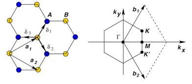
Fig. 1. Graphene honeycomb lattice and its Brillouin zone. Left: a1 and a2 are the lattice unit vectors, and δi, i=1,2,3 are the nearest-neighbor vectors. Right: The Dirac cones are located at the K and K’ points.

Phonon dispersion in graphene

The phonon dispersion of graphite plays a key role in interpreting its Raman spectra. In graphene there are 2 atoms per unit cell thus six phonon dispersion modes as seen in Fig. 2 out of which three are acoustic (A) and three are optical (O) phonon modes. For the three acoustic and three optical phonon modes, one is an out-of plane (oT) phonon mode and the other two are in-plane modes, one longitudinal (L) and the other one transverse (iTO). Thus, starting from the highest energy at the Γ point in the Brillouin zone the various phonon modes are labeled as LO, iTO, oTO, LA, iTA and oTA as shown in Fig. 2.

The optical phonons in the zone-center (Γ) and zone edge (K and K’) region are of particular interest, since they are accessible by Raman spectroscopy. The Γ point optical phonons are doubly degenerate with E2g symmetry for unperturbed graphene. The vibrations correspond to the rigid relative displacement of the A and B sub-lattices. This phonon mode is Raman active and responsible for the Raman G mode in graphene. The LO phonon branch near but away from the Γ point is not Raman active in a one- phonon process in defect free graphene, given that it has finite wave vector. However, in the presence of defects, it can be activated. Like the LO phonons around the Γ point, the TO phonon branch around the zone edge is accessible by a two-phonon Raman process, which gives rise to the G’ (also named 2D) mode.

Fig. 2. Calculated phonon dispersion relation of graphene showing the LO, iTO, oTO, LA, iTA, and oTA phonon branches.9

  • Raman scattering mechanism in graphene

The most prominent features in the Raman spectra of monolayer graphene are the so-called G band appearing at 1582 cm−1 (graphite) and the G’ band at about 2700 cm−1 using laser excitation at 2.41 eV. In the case of a disordered sample or at the edge of a graphene sample, we can also see the so-called disorder-induced D-band, at about half of the frequency of the G band (around 1350 cm−1 using laser excitation at 2.41 eV).

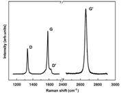
Fig. 3. Raman spectrum of a graphene edge, showing the main Raman features, the D, G and G’ bands taken with a laser excitation energy of 2.41 eV.

The G-band (for graphite) in the first-order Raman spectrum, corresponds to the optical mode vibration of two neighboring carbon atoms on a sp2-hybridized graphene layer. There is a tangential stretching of the σ bonds along the plane giving rise to the Raman G peak, which is one phonon intra-valley scattering process at the Γ point.

The double-resonance (DR) process shown in the center and right side of Fig. 4 begins with an electron of wave-vector k around K absorbing a photon of energy Elaser. The electron is inelastically scattered by a phonon or a defect of wavevector q and energy Ephonon to a point belonging to a circle around the K point, with wavevector k+q. The electron is then scattered back to a k state, and emits a photon by recombining with a hole at a k state. In the case of the D band, the two scattering processes consist of one elastic scattering event by defects of the crystal and one inelastic scattering event by emitting or absorbing a phonon, as shown in Fig. 4. In the case of the G’-band, both processes are inelastic scattering events and two phonons are involved.

The triple-resonance process can occur by both scattering of electrons and holes and the recombination happens at the inequivalent K’ point with respect to K point which generates the photon.

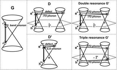
Fig. 4. (Left) First-order G-band process and (Center) one-phonon second-order DR process for the D-band (intervalley process) (top) and for the D-band (intravalley process) (bottom) and (Right) two-phonon second-order resonance Raman spectral processes (top) for the double resonance G process, and (bottom) for the triple resonance G band process (TR) for monolayer graphene. For one-phonon, second-order transitions, one of the two scattering events is an elastic scattering event. Resonance points are shown as open circles near the K point (left) and the K point (right).10

  • Raman studies of the number of graphene layers and stacking orders

The G’ features like position, line width and intensity are dispersive with the number of layers ‘n’ of the graphene layer, as shown in Fig. 5. This is attributed to the evolution of the bands of the mono-layer, bi-layer and few-layer graphene structures. These dependences can be used to characterize the number of graphene layers ‘n’ in few layer graphene samples.

The G’ band for 1-LG at room temperature exhibits a single Lorentzian feature with a full width at half maximum (FWHM) of 24 cm−1. For bilayer graphene with Bernal AB layer stacking, both the electronic and phonon bands split into two components. Four different DR processes11 can happen in bilayer case. Thus Raman spectra of a 2-LG sample with AB stacking can be fitted with four Lorentzians, each with a FWHM of24 cm−1. Using group theory analysis for a trilayer graphene, the number of allowed Raman peaks in the G’ band is fifteen. Due to the small energy separations of many of these fifteen transitions, experimentally it is found that the lineshape can be fitted with less peaks and the minimum number necessary to correctly fit the G’ is six. The high frequency side of the G’ band comes to dominate starting from 4-LG to HOPG. The G’ band is a convolution of peaks along the entire kz axis.


Fig. 5. The measured G’ Raman band with 2.41 eV laser energy for (a) 1-LG, (b) 2-LG, (c) 3-LG, (d) 4-LG, (e) HOPG and (f) turbostratic graphite. The splitting of the G’ Raman band opens up in going from mono- to three-layer graphene and then closes up in going from 4-LG to HOPG.10

The identification of the number of layers by Raman spectroscopy is well established only for graphene samples with AB Bernal stacking. In the case of randomly rotation stacking like turbostratic graphite, Raman shows a G’ band that is a single Lorentzian as in monolayer graphene but with a larger FWHM OF ~45-60 cm-1 and much smaller IG’/IG. This is due to the absence of an interlayer interaction between the graphene planes.

Recently, Intravalley R’ peak centered at1625 cm-1 is observed in randomly produced bilayer graphene due to a rotational-induced intervalley DR mechanism.12 Its properties depend on the mismatch rotation angle and can be used as an optical signature for superlattices in bilayer graphene.

  • Substrate effect

Clear understanding of the substrate effect is important for the potential device fabrication of graphene. Micromechanically cleaved monolayer graphene on standard SiO2 (300 nm)/Si, single crystal quartz, Si, glass, PDMS, and NiFe has been studied by Raman spectroscopy. It was found that G peak and G’ peak position and their FWHM have very small difference. The interaction between micromechanically cleaved graphene sheets and different substrates is not strong enough to affect the graphene sheets. G-band is made up of the long-wavelength optical phonons (TO and LO), and the out of plane vibrations in graphene are not coupled to this in-plane vibration. However, Raman of epitaxial graphene on SiC shows a big blueshift, which might due to strain effect and doping from substrate.


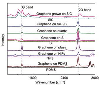
Fig. 6. The Raman spectra of monolayer graphene on different substrates as well that of epitaxial monolayer graphene on SiC.13

  • Graphene edges

Graphene edges are of particular interest, since their chirality determines the electronic properties. The edge is either formed by carbon atoms arranged in the zigzag or armchair configuration as shown in Fig. 7. Zigzag edges are composed of carbon atoms that all belong to one and the same sublattice, whereas the armchair edge contains carbon atoms from either sublattice. For a zigzag edge the momentum can only be transferred in a direction dz which does not allow the electron to return to the original valley in reciprocal space as shown in Fig. 7. Thus zigzag edges do not produce D peak in Raman spectroscopy. In graphene with perfect edges, if two edges form an angle of 120°, they should be the same. In contrast, an angle of 90 or 150° implies a change. In order to confirm this theory, Casiraghi14 carried out a detailed Raman investigation of graphene flakes with well-defined edges oriented at different crystallographic directions. The D to G ratio at the edge is never null due to some disorder at the edges.

Fig. 7. Raman double resonance mechanism in graphene and at the edge. (a) Atomic structure of the edge with armchair (blue) and zigzag (red) chirality. (b) Double resonance mechanism of the defect induced D peak. (c) First Brillouin zone of graphene and the double resonance mechanism in top view.15

By using carbo-thermal of SiO2 to SiO, Krauss15 able to make hexagonal holes with pure graphene zigzag edges. G peak appeared in both cases of round holes with mixture of zigzag and armchair edges and hexagonal holes with pure edge, while higher D peak intensity was shown in the vicinity of round holes. To rule out the random case, this was confirmed by statistic data.

Fig. 8. AFM images and Raman maps of graphene flakes containing round or hexagonal (top or bottom panels, respectively) holes. (a and d): AFM images of the round and hexagonal holes. (b and e) Intensity map of the Raman G peak. The G peak intensity is uniform across each flake except at the locations of the holes. These holes appear black (no graphene). The region where the AFM image was taken has been demarcated by a square. (c and f) Intensity map of the disorder-induced D peak. The D peak intensity is high in the vicinity of round holes (c). On the contrary, the D peak intensity is not enhanced near the hexagonal holes in (f).15

  • Graphene nanoribbons

Comparing to bulk graphene material, graphene nanoribbons (GNRs) are becoming more interested in transistors applications and quantum confinement study. GNRs have been predicted to behave as a semiconductor with a bandgap which is determined by ribbon width and chirality. A ribbon with zigzag configuration on either edge has an almost flat energy band at the Dirac point giving rise to a large peak in the density of states. The charge density for these states is strongly localized on the zigzag edge sites. Nanoscale spintronic devices have been dreamed up to utilize such unique features. Armchair devices are particularly suitable candidates for spin quantum bits.

Optical characterization of newly emerging properties of GNRs has been rare. In particular, Raman spectroscopy has not been systematically investigated on GNRs. As results shown in graphene edge studying, we can expect the D peak will show up in the nanoribbons with disorder edges. Ryu16 found the G peak became lower and broader as the width decreased as shown in Fig. 9. Disparity was shown in G’ peak for nanoribbons with one monolayer and bilayer graphene, which can be used to distinguish the layer numbers of nanoribbons. The change in G peak does not surprise us since its intensity is proportional to the number of sp2 bonds. Since the laser spot (can be as small as 400 nm) are much bigger than the width of nanoribbons, the smaller the width the lesser area of graphene was detected in Raman.

Fig. 9. Raman spectra of GNR sets with different ribbon width at 632.8 nm excited energy. The bands at 1450 and 1650 cm-1 are due to underlying Si and a plasma line of the excitation laser, respectively.16

Recently, a splitting of G at 1583 cm-1 and G+ at 1594 cm-1 was observed for H-terminated Z-GNRs, and a model was proposed to explain the dependence of I(G)/I(G+) on nanoribbon width.17 An individual Z-GNR has two spate portions: one is the edge-states affected portion (marked with red in Fig. 10.), contributing to G(softened E2g-modeG); the other is the center portion (marked with blue in Fig. 10.), contributing to G+ (intrinsic E2g-mode G+). When the nanoribbon width decreased, edge portion kept unchanged but central portion decreased, which decreased the I(G)/I(G+) as shown in Fig. 10.

Fig. 10. Width dependence of the relative intensity G/G+. (A) AFM images of GNRs with nearly perfect zigzag edge at different widths after nanopads removing. (B) Raman spectra for these Z-GNRs at different widths. (C) Fitted width dependence of the relative intensity G/G+. (D) Schematic of two-component Z-GNR: edge affected part (softened E2g-mode G, as shown in red) and perfect bulk part (intrinsic E2g-mode G+, as shown in blue).17

  • Summary

Raman spectroscopy has been established as a very versatile characterization tool not just to identify layer number but also towards measurement of defectivity, substrate effects and edge effects. The understanding of these properties is highly essential for the study of graphene for future carbon-based devices. While Raman spectroscopy has low spatial resolution limited by optical system when applied to characterization of graphene nanoribbons. Combining with other technique like inelastic electron tunneling spectroscopy can reveal more details on phonon modes thus get a better understanding of electronic properties of graphene nanoribbons.

  • Reference

1.    Lin, Y.-M. et al. 100-GHz transistors from wafer-scale epitaxial graphene. Science (New York, N.Y.)
327, 662 (2010).

2.    Banerjee, B.S.K. et al. Graphene for CMOS and Beyond CMOS Applications. Proceedings of the IEEE
98, (2010).

3.    Novoselov, K.S. et al. Electric field effect in atomically thin carbon films. Science (New York, N.Y.)
306, 666-9 (2004).

4.    Bonaccorso, F., Sun, Z., Hasan, T. & Ferrari, a. C. Graphene photonics and optoelectronics. Nature Photonics
4, 611-622 (2010).

5.    Son, Y.-W., Cohen, M.L. & Louie, S.G. Half-metallic graphene nanoribbons. Nature
444, 347-9 (2006).

6.    Tombros, N., Jozsa, C., Popinciuc, M., Jonkman, H.T. & van Wees, B.J. Electronic spin transport and spin precession in single graphene layers at room temperature. Nature
448, 571-4 (2007).

7.    Cortijo, A., Guinea, F. & Vozmediano, M.A.H. Geometrical and topological aspects of graphene and related materials. Arxiv preprint arXiv:1112.2054 1-34 (2011).at <http://arxiv.org/abs/1112.2054&gt;

8.    Bolotin, K. et al. Ultrahigh electron mobility in suspended graphene. Solid State Communications
146, 351-355 (2008).

9.    Dresselhaus, M.S., Jorio, a. & Saito, R. Characterizing Graphene, Graphite, and Carbon Nanotubes by Raman Spectroscopy. Annual Review of Condensed Matter Physics
1, 089-108 (2010).

10.    Ma lard, L.M., Pimenta, M. a., Dresselhaus, G. & Dresselhaus, M.S. Raman spectroscopy in graphene. Physics Reports
473, 51-87 (2009).

11.    Malard, L. et al. Probing the electronic structure of bilayer graphene by Raman scattering. Physical Review B
76, 201401 (2007).

12.    Carozo, V. et al. Raman signature of graphene superlattices. Nano letters
11, 4527-34 (2011).

13.    Wang, Y.Y. et al. Raman Studies of Monolayer Graphene: The Substrate Effect. Journal of Physical Chemistry C
112, 10637-10640 (2008).

14.    Casiraghi, C. et al. Raman spectroscopy of graphene edges. Nano letters
9, 1433-41 (2009).

15.    Krauss, B. et al. Raman scattering at pure graphene zigzag edges. Nano letters
10, 4544-8 (2010).

16.    Ryu, S., Maultzsch, J., Han, M.Y., Kim, P. & Brus, L.E. Raman spectroscopy of lithographically patterned graphene nanoribbons. ACS nano
5, 4123-30 (2011).

17.    Yang, R., Shi, Z., Zhang, L., Shi, D. & Zhang, G. Observation of Raman g-peak split for graphene nanoribbons with hydrogen-terminated zigzag edges. Nano letters
11, 4083-8 (2011).

超越摩尔定律 | Beyond Moore’s Law

Pursuit of high performance computation is endless desire of human being. This desire has given birth to Silicon Valley previously mentioned, modern society and this article. Moors’ Law serves so well in scaling down of transistor and Dennard’s Scaling Theory as more technical guide until very recent. It is very interesting to look into how the skyscraper of computation built up from single transistor to integrated circuit to hardware system such as personal computer, big server, even supercomputer. It is a bottom-up process in which lower level gives solid support to higher level. As maturity of semiconductor industries, society focus shift upwards to levels where holds more innovation and chaos, namely, software and cloud computing. But semiconductor is still a trunk which feeds a whole bunch of branches. How to keep it evergreen? Here are the plans intrigued by Brian’s presentation.

Plan A: Transistor Scaling

Scaling is predicted down to 8 nm. Currently Intel reaches to 22 nm by introduction of tri-gate structure. 3D integration is kind of another way to scale. Stacking of heterogenous IC could give more functions and lower power consumptions per area.


IDF 2011


Plan B: Circuit and System Design

If the physical limit are approaching, here is the near term issue we can look into. Innovations are demanded to optimize IC performance, power and variability. Non-volatile memory and multi-core computation are promising.


Plan C: Exploratory Research

Exotic material such as nanotube, graphene and quantum dot, new device like spintronics, also quantum computation.


A magnetologic gate, which consists of graphene contacted by several magnetic electrodes.

Reference:

THE INTERNATIONAL TECHNOLOGY ROADMAP FOR SEMICONDUCTORS: 2010 UPDATE

硅谷传奇 | Silicon Valley

硅谷神话一再被提起从未真正了解,一直被模仿[1]但从未被超越。那里是科技圣地,引来多少朝拜者和取经人,那里是天堂,是不是人才都想往里挤。乔布斯的突然离去是一个时代的结束,这话被说滥了,但也不假,那在这之前又是什么样的时代呢,他又是在怎样的一个时代诞生的,这是一个深入了解硅谷历史的契机,那就先从扒开历史的外衣开始享受吧,抓住一个中心(技术),两个关键点(社区和金融制度),每个人都应该自己体验一下。

网上有很多相关资料,下面是我觉得比较好的,一定得点

Silicon Valley
硅谷发动机的历史
Secret History of Silicon Valley
A Chronological Timeline of Computer
The Myth Of Silicon Valley

还有相关书籍
History of Semiconductor_Engineering
Makers of the Microchip A Documentary History of Fairchild Semiconductor
The Silicon Valley of Dreams

关于硅谷不得不知的人物

   Father of Silicon Valley

Frederick Terman – Stanford Industrial Park

  搞了个科技园区,鼓励学生创立了HP,吸引了Shockley和很多其   他公司,反过来促进了斯坦福大学和伯克利大学的发展。


   Father of Transistor
William Shockley, Shockley Semiconductor Laboratory


充满个性的天才,在Bell实验室跟别人一起搞出了晶体管,获     得了诺贝尔奖,后来离开Bell来到硅谷创立了肖克利半导体实验   室,从东部招来了以下八位年轻科学家。

The Traitorous Eight (仙童八叛逆): Julius BlankVictor GrinichJean HoerniEugene KleinerJay LastGordon MooreRobert Noyce and Sheldon Roberts.

这是肖克利招来的八位年轻人,跟肖克利闹翻之后,他们离开了肖克利半导体实验室,创立了仙童半导体 (Fairchild Semiconductor)。后来仙童半导体里的员工跳槽创立了AMD,后来 Gordon Moore Robert Noyce创立了Intel.

乔布斯说:仙童半导体公司就象个成熟了的蒲公英,你一吹它,这种创业精神的种子就随风四处飘扬了。然后乔布斯就来了。

Father of Apple

Steve Jobs, 1955-2011


[1] Silicon Valleys Popping Up Here, There, Everywhere

美西旅行

这次我们的旅行路线是Albany-> Los Angeles(三天四夜)-> Las Vegas(一天半一夜)-> Grand Canyon(一天一夜)-> Bryce Canyon(一天一夜)-> Zion Canyon(一天一夜)-> Las Vegas(一天一夜)-> Albany/Baltimore,历时九天九夜,感慨良多。在此要特别感谢在LA包吃包住包玩的谢谢和梦梦,以及靠喝红牛一路开车来回各大峡谷的天天,没有你们此行恐怕不可为啊。

能找到的最长最全的California Coast Travel Guide加州海岸旅遊及周边国家公园攻略:原始地址,整理后的Word版Kindle版

骁骁同学提供的洛杉矶攻略:Word版

亭亭同学提供的拉斯维加斯攻略:Word版

天天计划的Grand Canyon攻略:Word版

企业家誓言| Entrepreneur’s Credo

Entrepreneur’s Credo

<Common Sense>, written in 1776 by Thomas Paine

《企业家》杂志首刊

I do not choose to be a common man,
It is my right to be uncommon…if I can,
I seek opportunity….not security.
I do not wish to be a kept citizen,
Humbled and dulled by having the state looking after me.

I want to take the calculated risk;
To dream and to build,
To fail and to succeed.
I refuse to barter incentive for a dole;
I prefer the challenges of life
To the guaranteed existence;
The thrill of fulfillment
To the state of calm Utopia.

I will not trade freedom for beneficence
Nor my dignity for a handout.
I will never cower before any master
Nor bend to any threat.

It is my heritage to stand erect,
Proud and unafraid;
To think and act for myself,
To enjoy the benefit of my creations
And to face the world boldly and say:
This, with God’s help, I have done.

译文:

我不会选择做一名普通人。
自命不凡是天赋人权——只要我能。
我寻求机遇,而非安稳。
我也从不愿去做顺民,
在国家的保障下变得卑躬沉沦。

我要尝试那精心的冒险;
去梦想也去创造,去失败也去成功。
我拒绝失去激励而获得救助;
我宁愿接受生活的挑战,不甘心保有确定的现状;
成就带来的欣喜远比乌托邦式的平静更令我向往。

我不会为福利而牺牲自由;
也不会为施舍而放弃尊严。
在任何大师面前我不会胆怯;
在任何威胁面前也决不屈服。

我的天性是昂然挺立,自豪无惧;
按照内心的方式敢想敢为。
我享受自我创造产生的果实;
坦然面对这个世界,然后说:
此生,拜上帝之助,我有所作为。

——————————————–

Charles Dickens <A Tale of Two Cities>

It was the best of times, it was the worst of times, it was the age of wisdom, it was the age of foolishness, it was the epoch of belief, it was the epoch of incredulity, it was the season of Light, it was the season of Darkness, it was the spring of hope, it was the winter of despair, we had everything before us, we had nothing before us, we were all going direct to Heaven, we were all going direct the other way–in short, the period was so. far like the present period, that some of its noisiest authorities insisted on its being received, for good or for evil, in the superlative degree of comparison only.

狄更斯同志的《双城记》译文:

那是最美好的时代,那是最糟糕的时代;那是智慧的年头,那是愚昧的年头;那是信仰的时期,那是怀疑的时期;那是光明的季节,那是黑暗的季节;那是希望的春天,那是失望的冬天;我们全都在直奔天堂,我们全都在直奔相反的方向–简而言之,那时跟现在非常相象,某些最喧嚣的权威坚持要用形容词的最高级来形容它。说它好,是最高级的;说它不好,也是最高级的。

Reference: <公司的力量>

The Commercialization of Graphene

Welcome Lady Gaga of Materials

Lady Gaga has the most followers on twitter. And graphene has the most followers today in condensed matter physics, even in materials. Definitely, graphene has become the lady gaga of materials after winning The Nobel Prize in Physics 2010. Lady Gaga recently released a new song “Born this way”, saying she is born a superstar.

My mama told me when I was young
We are all born superstars
I’m beautiful in my way
Cause God makes no mistakes
I’m on the right track baby
I was Born This Way

Is graphene a real superstar? Then what’s the next album?

Some reports about graphene:

The 10 strangest facts about graphene

Nokias future super material

EU: Graphene flagship

Why Graphene Won Scientists the Nobel Prize

Graphene technology moves closer

In fairy tales, third place is often the best: it’s usually the third casket that contains the treasure, and the third child who finds fame and fortune. And so it may be for graphene, the third and most recently discovered form of “new carbon”. Last year, graphene was the subject of around 3000 research papers and more than 400 patent applications. One of the world’s largest steel producers in Korean POSCO announced partnership with XG Sciences to advance graphene manufacturing recently. And companies ranging from IBM to Samsung are testing graphene electronics. The hype over graphene has reached such a pitch that a casual follower might wonder why it hasn’t conquered the technological world already.

“I’m beautiful in my way.” She is beautiful in her own way! Does everybody like Lady Gaga? Not really. So how can a miracle material satisfy all needs? No way. Although graphene has two predecessors to learn from about fabrication and commercialization, it still has its own problem.

First, how to mass-producing the graphene? The most available graphene product in market is graphene sheets. Because composite-quality graphene has the potential to be a lot cheaper, it is able to compete with current carbon nanotube and other materials. Although much of the early excitement around graphene centred on its semiconducting properties and exotic physics, the tons of material now being manufactured will not end up in advanced devices such as transistors. For large-area and high-quality graphene using in high-tech applications, people have successfully grown graphene on metal catalyst but transfer process is still a nightmare. Epitaxial growth on SiC seems to solve this problem, but it is too expensive. We are working to manufacture wafer-scale high-quality graphene.

Second, what is outlet of graphene? The reality is that these applications are still niche, says a senior scientist with Dow Chemical’s Ventures and Business Development Group in Midland, Michigan. As you can see in the following figure, graphene has a very bright future in touch screens, supercapacitors, fuel cells, batteries, sensors, high-frequency circuits and flexible electronics. These applications have attracted the undivided attention of start-up companies, however, large chemical companies have so far taken a more conservative approach. The discrepancy between the enthusiasm of the start-up companies and the conservatism of their larger counterparts is partly a matter of scale. Even though tens of tons is orders of magnitude beyond laboratory production scales, it is also orders of magnitude below industrial chemical company scales.

“Asking graphene to compete with silicon now is like asking a 10-year-old to be a concert pianist because we’ve been giving him piano lessons for the last six years.” Graphene will have its place, but it will just take longer than people think.

Market

The global graphene-based product market value will grow to $67 million in 2015, and $675.1 million in 2020, according to BCC Research’s new report, “Graphene: Technologies, Applications, and Markets” (Report ID: AVM075A). That’s a 58.7% five-year compound annual growth rate (CAGR).

Figure. Global market for graphene-based products, 2009-2020 ($ millions). SOURCE: BCC Research

Graphene-based capacitors: The largest product segment. 67.2% 5-year CAGR, from $26 million in 2015 to $340 million in 2020.

Structured materials: Second-largest segment. 39.1% 5-yr CAGR, from $17.5 million in 2015 to $91 million in 2020.

Graphene in displays: Shooting up from a negligible value in 2015, this segment will reach $43.8 million in 2020.

Graphene-based photovoltaics (PV): 36.1% 5-yr CAGR, from $7.5 million in 2015 to $35 million in 2020.

Thermal management graphene products: 8.4% CAGR, from $15 million in 2015 to $22.5 million in 2020.

Remaining graphene-using products will make up a $1 million industry in 2015, and should hit $142.8 million in 2020 (169.7% 5-yr CAGR). The commercial market for graphene-based products was essentially nonexistent 2009-2010, but BCC expects commercially significant graphene sales to crop up before 2015. The BCC report surveys emerging graphene technologies and applications, identifies significant commercial sales opportunities in the next 5-10 years, and shares quantitative estimates of potential sales.

Existing Companies

Country Company Location University Affiliation Group
US 3M
EU Amo GmbH Aachen, DE
US Angstron Materials (a Nanotek spin-off) Dayton, OH Wright State University I
EU Aixtron Herzogenrath, DE
BASF
Carben Semicon
US Cheaptubes Vermont III
US CVD Equipment Corp. Long Island, NY
Dow Chemical
UK Durham Graphene Science Durham, UK Durham University II
JP Fujitsu Laboratories
US GE
US General Motors Corp.
US Graphene Devices University at Buffalo
US Graphene Energy Austin, TX University of Texas I
US Graphene Frontiers University of Pennsylvania
UK Graphene Industries Manchester, UK University of Manchester II
US Graphene Laboratories Reading, MA Columbia University II
UK Graphene Research Manchester, UK University of Manchester
US Graphene Works Atlanta, GA Georgia Institute of Technology II
EU Graphenea San Sebastián
CN Harbin Mulan Foreign Economic Trade Corp.
HRL Laboratories
US IBM
US Intel
CN Jcnano Nanjing, Jiangsu Nanjing University I
CN Nano-Brother Lab Harbin, Heilongjiang Harbin Institute of Technology II
CN Nanointegris III
Nanosperse
Nanoteck Instruments III
Nupga
IN Quantum Materials Corporation
Reade
KR Samsung Electronics
CN Sinocarbon Materials Technology Taiyuan, Shanxi Chinese Academy of Sciences I
US Texas Instruments
Unidym
US Vorbeck Materials Corporation Jessup, MD Princeton University I
US Vulvox Long Island, NY III
US XG Sciences Lansing, MI Michigan State University II
CN Xiamen knano Graphene Technology Xiamen, Fujian Huaqiao University
US Xolve (formerly Graphene solutions) Platteville, WI University of Wisconsin II
CN XP Nano Materials Xiamen, Fujian III

References:

Richard Van Noorden, The trials of new carbon, Nature, 2011.
Michael Segal, Selling graphene by the ton, Nature, 2009.
Sanjay K. Aroraa, etc., Graphene SME Commercialization Strategies: A Cross-Country Comparison, 2011.
Andrew Baluch, etc., Patenting Graphene: Opportunities and Challenges, Nanotechnology Law & Business, 2008.

Peep at others’ bookshelf

Bookshelf of CEO of SEMATECH, Daniel Armbrust

The Man Behind the Microchip: Robert Noyce and the Invention of Silicon Valley.

Leslie Berlin…must read bio of one of the most influential leaders in semiconductors

The Innovator’s Dilemma.

Clayton Christensen…Insights into how success breeds failure

The Gorilla Game.

Moore, Johnson, and Kippola…How companies are valued in the market

Crossing the Chasm.

Geoffrey Moore…Moving technology through the valley of death

Who Says Elephants Can’t Dance.

Lou Gerstner…lessons learned from the IBM turnaround

Personal History.

Katherine Graham…Incredible life story of the woman behind the Washington Post

Execution.

Larry Bossidy and Ram Charan…The “how to” on getting things done

The World is Flat.

Thomas Friedman…Must read for understanding global forces

Competitive Strategy.

Michael Porter…A classic text on how to compete in business

You’re in Charge – Now What?

Thomas Neff and James Citrin…How to approach a new position

The Reckoning.

David Halberstam…Compelling history of the car industry

Where Good Ideas Come From.

Steve Johnson…Importance of clusters and centers

High Output Management.

Andy Grove…Management advice from an Intel legend

What Technology Wants.

Kevin Kelly…Reflections on technology directions and trends

Capitalism 4.0

Anatole K…Next phase of financial, industry and government partnership

Barbarians at the Gate

Brian Borroughs and John Helyar…Incredible story telling of RJR Nabisco and LBO’s

Visual Display of Quantitative Information, Envisioning Information, Beautiful Evidence.

Edward Tufte…Visualizing data and information to tell a story

Bookshelf of an outstanding researcher at IBM working on graphene electronic device, Yu-Ming Lin

Numerical recipe” by Cambridge Press

Introduction to Solid-State Physics” by Charles Kittle

Solid-State Physics” by Ashcroft/Mermin

Springer Handbook of Nanotechnology

Noise” by Van der Zeil

Several tour guides for travel in Europe, Spain, and France.

The Business School and MBA: Past, Present, and No future here

Were people taught in school to do business 200 years ago? No!
Did people know what MBA was 100 years ago? No!
Are we becoming stupid? No one admit.
Why are MBA everywhere nowadays? Because that’s the way of people living, you’ll find some traits you might have at the following lists.

You know you are an MBA when….

You ask the waiter what the restaurant’s core competencies are.

You decide to re-org your family into a ‘team- based organization.’

You refer to dating as test marketing.

You can spell ‘paradigm.’

You actually know what a paradigm is.

You understand your airline’s fare structure.

You write executive summaries on your love letters.

You think it is actually efficient to write a ten-page paper with six other people you do not know.

You believe you never have any problems in your life, just ‘issues’ and ‘improvement opportunities.’

You calculate your own personal cost of capital.

You refer to your previous life as ‘my sunk costs.’

Your three meals a day are a ‘morning consumption function’, a ‘noontime consumption function’, and an ‘even consumption function.’

You start to feel sorry for Dilbert’s boss.

You refer to divorce as ‘divestiture.’

Your favorite artist is the one who does the dot drawings for the Wall Street Journal.

None of your favorite publications have cartoons.

You account for your tuition as a capital expenditure instead of an expense.

You insist that you do some more market research before you and your spouse produce another child.

At your last family reunion, you wanted to have an emergency meeting about their brand equity.

You decided the only way to afford a house is to call your fellow alumni and offer to name a room after them if they help with the down payment.

Your ‘deliverable’ for Sunday evening is clean laundry and paid bills.

You use the term ‘value-added’ without falling down laughing.

Past:

Present:

Global MBA Rankings 2011

Current rank 3 year average rank School name Country Weighted salary (US$) Salary percentage increase
1 1 London Business School U.K. 145776 132
1 1 University of Pennsylvania: Wharton U.S.A. 171551 123
3 3 Harvard Business School U.S.A. 170238 116
4 5 Insead France / Singapore 147883 108
4 5 Stanford University GSB U.S.A. 183260 115
6 10 Hong Kong UST Business School China 133334 142
7 6 Columbia Business School U.S.A. 163407 117
8 7 IE Business School Spain 149584 136
9 11 Iese Business School Spain 131890 138
9 9 MIT Sloan School of Management U.S.A. 158387 121
11 Indian Institute of Management, Ahmedabad (IIMA) India 174440 152
12 11 University of Chicago: Booth U.S.A 151373 109
13 13 Indian School of Business India 134406 187
14 14 IMD Switzerland 145846 89
15 13 New York University: Stern U.S.A. 138865 119
15 17 Yale School of Management U.S.A. 146959 133
17 16 Ceibs China 126315 155
18 15 Dartmouth College: Tuck U.S.A. 155020 113
18 22 HEC Paris France 122828 106
20 21 Duke University: Fuqua U.S.A. 136563 107
21 19 Esade Business School Spain 125346 128
21 21 Northwestern University: Kellogg U.S.A. 143365 100
23 National University of Singapore School of Business Singapore 100456 140
24 25 University of Michigan: Ross U.S.A. 137189 104
25 28 University of California at Berkeley: Haas U.S.A. 144790 87
26 21 University of Cambridge: Judge U.K. 137199 101
27 21 University of Oxford: Saïd U.K. 132905 102
28 35 SDA Bocconi Italy 110186 123
29 34 Manchester Business School U.K. 116100 111
30 33 Cornell University: Johnson U.S.A. 140273 107
31 31 UCLA: Anderson U.S.A. 137726 106
32 38 City University: Cass U.K. 124006 90
33 28 Nanyang Business School Singapore 104952 121
34 32 Cranfield School of Management U.K. 132059 89
35 34 Australian School of Business: AGSM Australia 123520 99
36 29 Rotterdam School of Management, Erasmus University Netherlands 107969 91
37 36 Imperial College Business School U.K. 115563 92
38 32 Emory University: Goizueta U.S.A. 120835 105
38 39 Georgetown University: McDonough U.S.A. 127539 108
40 42 University of Maryland: Smith U.S.A. 110931 105
41 42 Carnegie Mellon: Tepper U.S.A. 127078 100
41 31 Lancaster University Management School U.K. 110526 95
41 33 University of Virginia: Darden U.S.A. 130788 102
44 47 Rice University: Jones U.S.A. 117812 104
44 52 Texas A & M University: Mays U.S.A. 108435 116
46 51 University of Illinois at Urbana-Champaign U.S.A. 102947 121
46 46 University of Toronto: Rotman Canada 98760 87
46 47 University of Western Ontario: Ivey Canada 104327 97
49 50 University of Texas at Austin: McCombs U.S.A. 119298 93
49 51 York University: Schulich Canada 87849 94
51 55 Vanderbilt University: Owen U.S.A. 115194 105
52 49 University of Rochester: Simon U.S.A. 111226 110
53 56 Melbourne Business School Australia 111621 77
53 66 University of California at Irvine: Merage U.S.A. 101495 113
55 70 Durham Business School U.K. 101181 89
55 72 Vlerick Leuven Gent Management School Belgium 105484 87
57 McGill University: Desautels Canada 92937 97
58 46 Warwick Business School U.K. 109311 66
59 Pennsylvania State University: Smeal U.S.A. 110085 88
60 73 University of Cape Town GSB South Africa 140896 76
61 84 Hult International Business School U.S.A. / U.K. / U.A.E. / China 107079 87
62 51 University of North Carolina: Kenan-Flagler U.S.A. 114650 88
63 75 Wisconsin School of Business U.S.A. 106523 100
64 76 Arizona State University: Carey U.S.A. 98862 96
64 Ipade Mexico 96729 139
64 64 University of Iowa: Tippie U.S.A. 92658 119
64 60 University of Southern California: Marshall U.S.A. 116448 86
68 75 Birmingham Business School U.K. 97119 87
68 62 Boston University School of Management U.S.A. 104796 99
68 SP Jain Center of Management Dubai / Singapore 81512 106
68 67 Thunderbird School of Global Management U.S.A. 102984 98
72 73 Ohio State University: Fisher U.S.A. 100191 95
73 63 Indiana University: Kelley U.S.A. 112676 86
74 70 Boston College: Carroll U.S.A. 111114 83
74 69 Purdue University: Krannert U.S.A. 100252 94
74 55 University of Strathclyde Business School U.K. 103801 87
77 Incae Business School Costa Rica 89212 106
78 92 University College Dublin: Smurfit Ireland 105354 72
78 81 Wake Forest University: Babcock U.S.A. 108520 110
80 78 University of British Columbia: Sauder Canada 88894 72
80 76 University of Notre Dame: Mendoza U.S.A. 107914 101
80 71 University of South Carolina: Moore U.S.A. 91297 93
83 University of California: Davis U.S.A. 100875 93
84 91 Babson College: Olin U.S.A. 113392 85
84 Eada Spain 90881 86
86 College of William and Mary: Mason U.S.A. 98238 102
86 77 University of Washington Business School: Foster U.S.A. 107118 73
88 85 SMU: Cox U.S.A. 103150 89
88 90 University of Edinburgh Business School U.K. 102068 64
90 89 Bradford School of Management/TiasNimbas Business School U.K. / Netherlands / Germany 84274 81
91 89 Brigham Young University: Marriott U.S.A. 99557 102
92 Pepperdine University: Graziadio U.S.A. 100000 103
93 University of Georgia: Terry U.S.A. 101750 82
94 Leeds University Business School U.K. 95498 70
94 78 University of Florida: Hough U.S.A. 93317 85
96 Politecnico di Milano School of Management Italy 74184 94
97 Georgia Institute of Technology U.S.A. 105000 60
98 IAE Business School Argentina 72797 82
99 Kaist College of Business South Korea 98927 74
100 EM Lyon Business School France 89246 53

Useful links:

Business school rankings

Global MBA Rankings 2011

Online MBA 2011 Listing

No future?

Maybe somewhere else. Maybe you should learn MBA to know.

希腊神话引发的命名学

周末了,要搞点非学术的东西,晚上看了亚历山大大帝,一个征服强大波斯帝国并把马其顿帝国扩张到印度边界的天才将领,一个被荣耀所困一生的男人。他的成功是举世无双的,他的失败都要高于其他人的成功。他师从亚里士多德,他爸是腓力二世,难道腓力牛排由此命名?他25岁时就率领军队打败了大流士三世,征服了波斯,而我在美国师夷长技,人生的差距啊。毫无疑问他与生俱来的胆识和欲望是不可匹敌的,但一生专注于征服和战争,使他无法分心去巩固帝国霸业,在其死后帝国迅速分崩离析,而他的死也成为千古谜团,只有33岁。他的悲剧就是和不理解自己的人们在一起,孤独和烦躁日积月累,因为他是世上最追求自由的人。他的偶像是阿喀琉斯,就是脚后跟软的战神,也是催生了微积分的神[1]。这些奇怪的名字再次唤起我对古希腊神话的兴趣,而且之前的好莱坞大片《诸神之战》和正在上映的《雷神之锤》估计会引发一股希腊神话热,所以就稍微研究了下。希腊神话已经渗透到大众生活中的方方面面,日常语言,文学,艺术,电影,音乐,给孩子取名字等等。其中充满着各种美学,乱伦与暴力是人类精神的源头和心灵的摇篮。小时候看过一些中文译本的希腊神话,里面的名字叫那个复杂,还是英文的短一些。以下是按时间顺序回顾不同阶段的希腊诸神。如果以后要取名字,这个肯定用得着,认真看的话会发现好多名字是那么的熟悉。

  • 混沌之神 Khaos/Chaos
  • 五初神及后代

宇宙之初,只有卡俄斯,他是一个无边无际、一无所有的空间。随后诞生了地母神该亚(Gaia)、地狱深渊神塔耳塔洛斯(Tartarus)、黑暗神俄瑞波斯(Erebus)、黑夜女神尼克斯(Nyx)和爱神厄洛斯(Eros)世界由此开始。

该亚(Gaea):大地女神,卡俄斯之女。大地的本体,她诞生了天空乌拉诺斯(Ouranos)、海洋彭透斯(Pontus)和山脉乌瑞亚(Ourea)。
接着她又和她两位儿子生了许多神。和乌拉诺斯生了十二位提坦(Titans)分别代表了世界最初的些事物(曰、月、天、时间、正义、记忆等)和彭透斯生了五个孩子分别代表了不同的海。她算得上是众神之母(是奥林匹斯神的始祖)。
塔耳塔洛斯(Tartarus):地狱深渊神,卡俄斯之子。五大创世神之一,可以说是地狱冥土的创造者,深渊的本体。
他出生在大地该亚之后,在该亚的下面,后来和该亚生了该亚最小儿子的就是怪物提丰(Typhon)。他是一个无形的深渊,位于世界的最底端,此后他是关押妖魔怪物和一些神坻的地方。宙斯就把一些提坦神关押在塔耳塔洛斯
厄瑞波斯(Erebus):黑暗神,卡俄斯之子。五大创世神之一,塔耳塔洛斯诞生后,在塔耳塔洛斯之处以上(地下/该亚之下)诞生。黑暗的化身与本体,位于大地(该亚)与冥土之间。他和她妹妹黑夜女神尼克斯(Nyx)生了三位古老的神坻,他们是:
太空之神埃忒耳 (Aether)、白昼之神赫莫拉 (Hemera)和冥河的渡神卡戎(Charon)。
尼克斯(Nyx):黑夜女神,卡俄斯之女。五大创世神之一,厄瑞波斯诞生后在大地(该亚)之上诞生。黑夜的化身和本体,她是一位古老而强大的神坻,她不但同他哥哥生了三个孩子外还独自一人生了一大批神
厄洛斯(Eros):爱神,卡俄斯之子。五大创世神之一,诞生在黑暗和黑夜之后。爱欲、生育及性欲的化身。是他促生了诸神的生育相爱,他是一切爱欲的化身(包括同姓、异性)
乌拉诺斯(Uranus):天之神。该亚的长子和丈夫,第一任神王。被他儿子推翻。
彭透斯(Pontus):海神,该亚之子和情人,最早的海神。
乌瑞亚(Ourea):山神,该亚诸子。

  • 十二泰坦

克洛诺斯(Cronus):该亚与乌拉诺斯的十二个提坦神儿女中最年幼者。天、空间神,推翻父神而成为第二任神王。。
瑞亚(Rhea):十二坦之一,时光女神。克洛诺斯的妻子第二任神后。
俄刻阿诺斯(Oceanus):十二提坦之一,大洋河流之神。生育了地球上所有的河流及三千海洋女神。
泰西斯(Tethys):十二提坦之一,沧海女神;俄刻阿诺斯之妻。
许配利翁(Hyperion):十二提坦之一,光明太阳之神。太阳,月亮和黎明之父。
提亚(Thea):十二提坦之一,宝物、光及视力女神;许配利翁之妻。
摩涅莫绪涅(Mnemosyne):十二提坦之一,记忆之神.宙斯第五位妻子九缪斯之母。
伊阿佩托斯(Iapetus):十二提坦之一。普罗米修斯,厄毗米修斯和阿忒拉斯之父。
克瑞斯(Crius):十二提坦之一,生长之神。
忒弥斯(Themis):十二提坦之一,秩序和正义女神.宙斯第二位妻子时序三女神之母
菲碧(Phoebe):也称福伯或福碧,十二提坦之一,月之女神勒托与阿斯特瑞亚之母。
科俄斯(Coeus):十二提坦之一,暗与智力之神。菲碧的老公。
普罗米修斯(Prometheus):伊阿佩托斯之子。最有智慧的神之一,被称为“先知者”。人类的创造者和保护者。因触怒宙斯被锁在高加索山上,每日有秃鹰啄食其肝脏,然后又长好,周而复始。后被赫拉克剌斯救出。
厄毗米修斯(Epimetheus):普罗米修斯的兄弟。最愚笨的神之一,被称为“后知者”。因接收了宙斯的礼物——潘多拉为妻,结果从“潘多拉之盒”中飞出了疾病,罪恶等各种灾难降临人间。
阿忒拉斯(Atlas):普罗米修斯的另一个兄弟。最高大强壮的神之一。因反抗宙斯失败而被罚顶天。
墨提斯(Metis):智慧女神,俄克阿诺斯之女,宙斯的第一位妻子,雅典娜的母亲
欧律诺墨(Eurynome):海洋女神,俄克阿诺斯之女,宙斯第三位妻子,美惠三女神之母
勒托(Leto):暗夜女神,克俄斯与菲碧之女,宙斯第六位妻子阿尔忒密斯与阿波罗之母

  • 奥林匹斯主神

宙斯(Zeus):克洛诺斯和瑞亚之子;掌管天界,是第三任神王;以贪花好色著名。
赫拉(Hera):宙斯的姐姐和夫人,美丽的天后;婚姻的保护神,尤其是已婚的女人的保护者。
波塞冬(Poseidon):宙斯的兄长;掌管大海;脾气暴躁,贪婪。
哈得斯(Hades):宙斯的兄长;掌管冥府,同时也是财富之神;有一顶可以隐身的帽子;残忍,可怕,但很守信。
德墨忒尔(Demeter):克洛诺斯和瑞亚之女,丰产、农林女神。宙斯的二姐与第四位妻子。
赫斯提亚(Hestia):
家灶及火焰女神,她是克罗诺斯郁瑞亚最大的孩子宙斯的大姐,掌万民的家事。三位处女神明之一。在希腊神话中,并没有详尽的记载。她是位贞洁处女女神。
阿瑞斯(Ares):宙斯与赫拉之子;战争之神;粗暴而嗜血,但并非真正的勇士。
雅典娜(Athena):宙斯与美狄丝结合的产物;智慧女神和女战神;她是智慧,理智和纯洁的化身。
阿波罗(Apollo):宙斯和勒托之子,和阿耳忒弥斯是双生弟弟;射术、音乐神,光明神;全名为福玻斯·阿波罗(Phoebus Apollo)。
阿弗洛狄忒(Aphrodite):爱,美和欲望之神;从海中的泡沫中生出。
赫尔墨斯(Hermes):宙斯和迈亚之子;众神中最快者;盗窃者的守护神,商业之神,黄泉的引导者。
阿尔忒弥斯(Artemis):宙斯和勒托之女,与阿波罗是双生姐姐;美丽的女猎神和月神,青年人的保护神。
赫淮斯托斯(Hephaestus):宙斯与赫拉之子,神中唯一丑陋者,但妻子却是爱与美之神阿佛洛狄忒;火和锻造之神,为众神制造武器和铠甲;铁匠和织布工的保护神。
其他神祗
埃忒尔(Aether):太空神,厄瑞波斯与尼克斯之子。
赫墨拉(Hemera):白昼神,厄瑞波斯与尼克斯之女。
卡戎(Charon):冥河渡神,厄瑞波斯与尼克斯之子。
塔那托斯(Thanatos):死神;黑夜女神尼克斯之子。
修普诺斯(Hypnus):睡神;黑夜女神尼克斯之子。
厄里斯(Eris):不和之女神;黑夜女神尼克斯之女;,最喜挑起不和,最著名的成就是挑起了“特洛伊之战”。
莫伊莱(Moerae):命运三女神;黑夜女神尼克斯之女。克罗托(Clotho)纺织生命之线,拉刻西斯(Lachesis)决定生命之线的长度,阿特洛波斯(Atropos)切断生命之线。
摩洛斯(Morus):厄神、命数神;黑夜女神尼克斯之子。
刻耳(Ceres):鬼神;黑夜女神尼克斯之子
摩墨斯(Momus):嘲神; 黑夜女神尼克斯之子
卡尔(Ker):破坏毁灭神;黑夜女神尼克斯之子
俄匊斯(Oizys):忧神;黑夜女神尼克斯之子
涅墨西斯(Nemesis):义愤报应女神;黑夜女神尼克斯之女
阿帕忒(Apate):骗神;黑夜女神尼克斯之女
菲罗忒斯(Philotes):淫神(性欲淫乱之神);黑夜女神尼克斯之子
革剌斯(Geras):年龄女神黑夜女神尼克斯之女
阿斯忒瑞亚(Asteria):星夜女神,暗夜女神勒托之妹。三位夜之女神中,尼克斯是夜之本体的化身,而勒托与阿斯忒里亚姐妹乃是夜的两种不同出现:勒托象征无星无月的黑暗之夜,阿斯忒瑞亚则对应星光璀璨之夜。
赫卡忒(Hecate):幽冥和魔法女神,世界的黑暗面就象征着她。冥后的侍女。星夜女神阿斯忒瑞亚和破坏神珀耳塞斯的独身女。
尼弥西斯(Nemesis):复仇女神;专门惩罚不法之徒。
赫利俄斯(Helios):太阳神,许配里翁与提亚之子,月女神塞勒涅与曙光女神厄俄斯之兄。
塞勒涅Selene):月亮女神,许配里翁与提亚之女,太阳神赫利俄斯与曙光女神神厄俄斯之姐妹。
厄俄斯(Eos):黎明女神,许配里翁与提亚之女,太阳神赫利俄斯与月亮女神塞勒涅之姐妹。
珀耳塞福涅(Persephone):冥后,德墨忒耳之女春神;冥王哈德斯之妻。
厄洛斯(Eros):小爱神,阿佛洛狄忒和赫尔墨斯或阿瑞斯之子。他的“武器”是魔力标枪或弓箭。被射中的人将会对其见到的第一个异性产生不可抑制的爱情。
赫柏(Hebe):宙斯和赫拉之女;青春女神,是奥林匹斯山的斟酒女郎。后嫁给赫拉克剌斯为妻。
潘(Pan):牧神,赫尔墨斯之子;长着一对羊角和一双羊蹄。是个出色的作曲家和笛子演奏家。快乐和顽皮好色的神,经常和山林的女仙们跳舞。然而,由于他丑陋的外表,总找不到老婆。
美惠三女神(TheGraces):宙斯和欧律诺墨的女儿;众神的歌舞演员,为人间带来诸美;分别是阿格莱亚(Aglaia,光辉女神),欧佛洛绪涅(Euphrosyne,欢乐女神),塔利亚(Thalia,激励女神)。
艺术女神(TheMuses):宙斯和摩涅莫绪涅的女儿们,共有九人;亦称为缪斯或庇厄利亚的女神们(Pierides),因她们生于庇厄利亚地方。她们是卡拉培(Calliope,雄辩和叙事诗),克利欧(Clio,历史),乌拉妮娅(Urania,天文),梅耳珀弥妮(Melpomene,悲剧),塔利亚(Thalia,喜剧),特普斯歌利(Terpsichore,舞蹈),依蕾托(Erato,爱情诗),波利海妮娅(Polyhymnia,颂歌),优忒毗(Euterpe,抒情诗)。
厄里倪俄斯(theErinnyes):复仇女神,又被称为欧墨尼得斯(Eumenides)。无情地报复犯罪者,直到其死亡。对犯弑母大罪的人尤其严厉。共有三人,提希丰(Tisiphone),美嘉拉(Megaera),阿耳刻托(Alecto)。她们从乌拉诺斯的血液中诞生。一说是乌拉诺斯的精血溅飞在该亚身上,该压所生。
普利俄阿德斯(ThePleiades):阿忒拉斯的七个如花似玉的女儿。分别是伊莱卡(Electra),迈亚(Maia),塔吉忒(Taygete),阿耳刻悠妮(Alcyone),美罗珀(Merope),塞莱诺(Celaeno),丝黛罗普(Sterope)。其中迈亚是赫耳墨斯的妈。
时序女神[]/url(Hours):宙斯和忒密斯之女,共三人——欧诺弥亚(秩序),狄刻(公正),厄瑞涅(和平)。
塔拉萨(Thalassa):海面女神,埃特拉与赫莫拉的女儿,彭透斯的妻子。
涅柔斯(Nereus):彭透斯和该亚长子,外号“海中老人”。是个知识渊博,真诚善良的老神仙。
多丽斯(Doris):俄克阿诺斯之女,三千海洋女神之一。涅柔斯之妻。
陶玛斯(Thaumas):奇观之海神,彭透斯和该亚的孩子。
福耳库斯(Phorcys):破坏之海神,彭透斯和该亚的孩子。
刻托(Ceto):危险之海神,彭透斯和该亚的孩子。
欧律比亚(Eurybia):力量之海神,彭透斯和该亚的孩子。
忒提丝(Thetis):涅柔斯的女儿之中最贤慧者。
安菲特里忒(Amphitrite):海后,涅柔斯之女,波赛东之妻
海神女(TheNereids):涅柔斯和多丽斯的五十个可爱女儿。他们是1、普洛托(Ploto);2、欧克拉忒(Eucrante);3、萨俄(Sao)4、安菲特里忒(Amphitrite);5、奥多拉(Eudora);6、忒提斯(Thetis);7、伽勒涅(Galene);8、格劳刻(Glauce);9、库姆托厄(Cymothoe);10、斯佩俄(Speo);11、托厄(Thoe);12、哈利厄(Halie);13、帕西忒亚(Pasithea);14、厄拉托(Erato);15、欧里刻(Eunice);16、墨利忒(Melite);17、欧利墨涅(Eulimene);18、阿高厄(Agaue);19、多托(Doto);20、普罗托(Proto);21、斐鲁萨(Pherusa);22、狄拉墨涅(Dynamene);23、尼萨亚(Nisaea);24、阿克泰亚(Actaea);25、普洛托墨狄亚(Protomedea);26、沲瑞斯(Doris);27、潘诺佩亚(Panopea);28、伽拉泰亚(Galatea);29、希波托厄(Hipothoe);30、希波诺厄(Hipponoe);31、库摩多刻(Cymodoce);32、库摩(Cymo);33、厄俄涅(Eione);34、阿利墨德(Alimede);35、格劳科诺墨(Glauconome);36、蓬托波瑞亚(Pontoporea);37、勒阿革瑞(Leagore);38、欧阿革瑞(Euagore);39、拉俄墨狄亚(Laomedea);40、波吕诺厄(Polynoe);41、奥托诺厄(Autonoe);42、吕西阿娜(Lysianassa);43、欧阿涅(Euarne);44、普萨玛忒(Psamathe);45、墨尼珀(Menippe);46、涅索(Neso);47、欧波摩珀(Eupompe);48、忒弥斯托(Themisto);49、普罗诺厄(Pronoe);50、涅墨耳提斯(Nemertes)。
特里同(Triton):海神波塞冬和安菲特里忒之子;手拿个大海螺半人半鱼。
米诺斯(Minos):克里特国王;以严密的法治而闻名,因此死后成为冥府的判官之一;宙斯和欧罗巴的儿子。
拉达曼达斯(Rhadamanthys):米诺斯的兄弟,亦是冥府判官之一。
卡吕普索(Calypso):海上女神,阿忒拉斯的女儿;爱上了凡间的英雄俄底修斯,但由于宙斯的阻挠未能与其成婚。
阿刻罗俄斯(Achelous):河神,俄刻阿诺斯和泰西斯的诸子中最长者。众海妖塞壬之父。
阿尔库俄纽斯(Alcyoneus):天与地之子,最强大的巨人,在地上时不会被杀死。
阿玛耳忒亚(Amalthea):海中仙女,有一可从中取食物的牛角。河神阿刻罗俄斯的角被赫拉克剌斯折断后,她将自己的一个送给阿刻罗俄斯。
伊里丝(Iris):宙斯的使者;彩虹女神;人头鸟哈耳皮埃的妹妹。
琉喀忒亚(Leucothea):海中女神;波塞冬将俄底修斯的船打碎后,她曾搭救俄底修斯。
珀耳塞(Perse):俄刻阿诺斯与泰西斯之女,是赫利俄斯的妻子。
克吕墨涅(Clymene):俄刻阿诺斯与泰西斯的女儿。赫利俄斯的情人好像和若干个神都有过亲密关系,包括普罗米修斯和阿波罗等,并生育了不少子女。
喀耳刻(Circe):赫利俄斯和珀耳塞的女儿,是个女魔法师,能把人变为牲畜。
普洛透斯(Proteus):海中老人,变化无穷。
斯卡曼德洛斯(Scamander):河名,亦是河神名;又叫克珊托斯(Xanthus)
赫斯帕里得斯(Hesperides):即夜的女儿们;守卫该亚作为结婚礼物送给赫拉的金苹果树。
绪任克斯(Syrinx):山林女神,为潘所追求,化为芦苇。
帕拉斯(Pallas):特里同的女儿;雅典娜无意中杀死她,因纪念她,自己该名帕拉斯,自称为帕拉斯•雅典娜。
格劳克斯(Glaucus):海神,善做预言。
塔罗斯(Talos):巨人,青铜时代最后一人;守卫克里特岛。
墨诺提俄斯(Menoetius):冥王的牧人。
比亚(Bio):凶猛的化身,帕拉斯与与斯堤克斯河所生的儿子。
克拉托斯(Cratos):强力的化身,帕拉斯与斯堤克斯河所生的儿子,是”凶猛”的兄弟。
怪物
厄喀德那(Echidna):半人半蛇的怪物。生了许多著名的妖怪——如勒耳那水蛇,涅墨亚狮子,咯迈拉,斯芬克斯等。
戈耳工(Gorgons):福耳库斯与刻托的三个女儿,其中之一是墨杜萨。
克律萨俄耳(Chrysaor):波塞冬和墨杜萨所生的怪物,珀伽索斯的兄弟。
刻耳柏洛斯(Cerberus): 三头狗,堤丰和厄刻德那所生,把守地狱的大门。
拉冬(Ladon):看守金苹果的百首龙,刻托和福耳库斯所生。
弥诺陶洛斯(Minotaur):克里特岛上牛头人身的怪物,喜食人肉,尤其是童男童女;著名的克里特迷宫即为软禁它而建。
珀伽索斯(Pegasus):飞马;波塞冬与墨杜萨所生,当珀耳修斯割下墨杜萨的头时,与克律萨俄耳一起从墨杜萨头中跳出。
克律萨俄耳(Chrysaor):波塞冬与墨杜萨所生的怪物,飞马珀伽索斯的兄弟。
格莱埃(Graeae):福耳库斯和刻托的三个女儿,与戈耳工是姊妹;她们共有一只眼睛,一只牙齿。
许德拉(Hydra):堤丰和厄咯德拉所生的水蛇,有九个头,因住在勒耳那大泽,又称勒耳那大蛇。
喀迈拉(Chimaera):喷火的妖怪,为堤丰和厄喀德那所生,狮头,羊身,蛇尾。
斯库拉(Scylla):意大利和西西里海峡之间的海妖。
斯芬克斯(Sphinx):堤丰和厄喀德那所生的怪物,有翼,长着美女的头,和狮子的身子;因俄狄浦斯杀父,前往忒拜为害。
堤丰(Typhon):该亚和塔耳塔洛斯的最小儿子,极度恐怖的怪兽;又称为堤福俄斯(Typhoeus)。
塞壬(Siren):福耳库斯和一位缪斯的女儿。她们住在一个海岛上,以歌声诱惑并杀死路过的水手。
墨杜萨(Medusa):戈耳工之一;凡见到她头的人都将变成石头。
人类和半神人
潘多拉(Pandora):赫淮斯托斯用泥土造成的女人,众神赐与诸善。
厄帕俄斯(Epeius):希腊军中著名的巧匠,建造了木马。
厄瑞克透斯(Erechtheus):雅典王;该亚和赫淮斯托斯之子,由雅典娜抚养大。
厄特克勒斯(Eteocles):俄狄浦斯的儿子,抵抗攻打忒拜的七将,死于自己兄弟之手。
俄里翁(Orion):俊美而强壮的猎人,为阿忒拉斯的七个女儿所爱,死后变成猎户座。
俄耳甫斯(Orpheus):缪斯之一卡利俄珀的儿子;他能以琴声使山林,岩石移动,使野兽驯服。死后成为天琴座。
伊俄(Io):是地中海地区某国公主,为宙斯所爱,将他变成小母牛,被赫拉派牛氓追逐,后在普罗米修斯的指引下逃脱。最后成为埃及的女神伊西丝(Isis)。
阿斯克勒皮俄斯(Asclepius):天医,阿波罗与克吕墨涅的儿子;为宙斯所杀。
布里塞伊丝(Briseis):特洛亚著名美女;为阿喀琉斯所俘虏,由于她的谜煞虿引起了希腊将帅不和。
欧罗巴(Europe):美丽的人间女子,为宙斯所引诱,是宙斯最著名的情人之一。
卡德摩斯(Cadmus):欧罗巴的哥哥;忒拜城的建立者。
卡帕纽斯(Capaneus):攻打忒拜的七雄之一。
卡珊德拉(Cassandra):普里阿摩斯和赫卡柏之女;是女预言家,曾预言了特洛亚的毁灭。
代达罗斯(Daedalus):全希腊最有名的建造大师,善于各种工艺技巧。
尼柔斯(Nireus):泉水女神的儿子,希腊将领中最英俊者。
皮拉(Pyrrla):厄庇墨透斯和潘多拉的女儿,丢卡利翁的妻子;唯一躲过宙斯洪水的两个人。
安菲阿剌俄斯(Amphiaraus):著名先知,攻打忒拜的七雄之一。
安菲翁(Amphion):宙斯的儿子;以竖琴的魔力建成了忒拜的宫殿。
安德洛玛刻(Andromache):赫克托耳的妻子,以对丈夫钟爱著称。
安提罗科斯(Antilochus):攻打特洛亚的希腊将领之一,以英俊勇敢著称,是阿喀琉斯的挚友之一。
丢卡利翁(Deucalion):普罗米修斯和克吕墨涅之子,皮拉的丈夫;宙斯发洪水毁灭人类时只留下他们俩。
伊卡洛斯(Icarus):代达罗斯之子;和父亲一起逃离克里特时,因飞近太阳,落水而死。
伊克西翁(Ixion):拉庇泰国王;因意图对赫拉无理,宙斯将他缚在旋转的车轮上,永远在冥土受罚。
伊阿西翁(Jasion):宙斯和海中某女神的儿子,他追求农业女神德米特耳,为宙斯所杀。
伊阿宋(Jason):夺取金羊毛的阿耳戈英雄的首领;美狄亚的丈夫。
西绪福斯(Sisyphus):人类中最狡猾者;死后在冥土受罚,永远推巨石上山,但将及山顶巨石又复落下。
克律塞伊丝(Chryseis):特洛亚方面阿波罗祭司的女儿,为阿伽门农俘虏,后者拒绝将她交还给其父,结果导致太阳神的报复。
克吕泰涅斯特拉(Clytaemnestra):阿伽门农的妻子,杀死了自己的丈夫,又被自己儿子所杀。
狄俄墨得斯(Diomedes):特洛亚战争中,希腊方面著名的大英雄。
希波墨冬(Hippomedon):攻打忒拜的七雄之一。
忒修斯(Theseus):雅典王;希腊神话中的著名大英雄之一。
忒勒玛科斯(Telemachus):奥德修斯的儿子;父亲从特洛亚战争中归来后,帮助父亲杀死所有求婚者.
忒拉蒙(Telamon):夺取金羊毛的阿耳戈英雄之一。
忒瑞西阿斯(Tiresias):忒拜先知,盲目,据说因无意中窥见雅典娜出浴而被判失明。
阿喀琉斯(Achilles):珀琉斯和海中女神忒提丝之子,浑身刀枪不入,唯一的弱点是脚踝;特洛亚战争中的希腊最伟大英雄。
阿德剌斯托斯(Adrastus):阿耳戈斯王;攻打忒拜的七将之一。
阿伽门农(Agamemnon):阿特柔斯之子;特洛亚战争中希腊方面的统帅。
阿尔刻提斯(Alcestis):珀利阿斯的女儿;以钟情丈夫著名,自愿代丈夫就死。
阿塔兰忒(Atalanta):伊阿索斯和克吕墨涅的女儿,美丽而野性的女猎手.
阿特柔斯(Atreus):珀罗普斯和希波达弥亚的儿子,坦塔罗斯的孙子.
欧律斯透斯(Eurystheus):珀耳修斯的孙子;赫拉克剌斯被罚为他做十二件大事.
拉奥孔(Laocoon):特洛亚城的阿波罗祭司,因他劝告特洛亚人警惕木马,雅典脑火怒, 派两条蛇将他咬死.
帕里斯(Paris):特洛亚王子;由于他诱拐天下第一美女海伦而引起特洛亚战争.
帕耳忒诺派俄斯(Parthenopaeus):阿德剌斯托斯的兄弟,攻打忒拜的七英雄之一.
帕特洛克洛斯(Patroclus):诺提俄斯之子;阿喀琉斯的密友;死于赫克托耳之手, 他的死使阿喀琉斯重新参战攻打特洛亚.
法厄同(Phaethon):赫利俄斯和克吕墨涅的儿子;因强驾太阳神车,从天上跌下致死.
波吕尼刻斯(Polynices):俄狄浦斯和伊俄卡斯忒的儿子;攻打忒拜的七英雄之一.
坦塔罗斯(Tantalus):宙斯的儿子,众神的朋友;因杀死儿子宴请天神,被罚入冥土永受饥渴之苦.
美狄亚(Medea):美丽的女魔法师,她帮助伊阿宋取得金羊毛,并嫁给他;后因伊阿宋移情别恋,亲手杀苏煞蛟己的两个儿子并设计杀死了伊阿宋的新欢.
珀利阿斯(Pelias):伊阿宋的叔叔,他篡夺了本应属于伊阿宋的王位.
珀琉斯(Peleus):阿耳戈英雄之一;忒提丝的丈夫,阿喀琉斯之父.
珀罗普斯(Pelops):坦塔罗斯之子;被其父做成菜肴给天神食用,后为命运女神复活.
珀涅罗珀(Penelope):奥德修斯忠贞的妻子;丈夫远征特洛亚失踪后,拒绝了所有求婚者, 一直等待丈夫归来.
珀耳修斯(Perseus):宙斯和达那厄的儿子;希腊神话中的大英雄之一.
辛尼斯(Sinnis):著名强盗,外号”扳松贼”,用两棵松树将旅人撕裂;波塞冬之子;为忒修斯所杀.
达玛斯忒斯(Damastes):著名强盗,外号”铁床贼”;没准儿也是波塞冬之子;为忒修斯所杀.
斯喀戎(Sciron):著名强盗,强迫旅人为他洗脚;差不多也是波塞冬之子;被忒修斯杀死.
埃厄忒斯(Aeetes):赫利俄斯和珀耳塞之子,喀耳刻之兄,美狄亚之父.
埃涅阿斯(Aeneas):阿佛洛狄忒的儿子,特洛亚英雄之一.
埃俄罗斯(Aeolus):希波忒斯之子,克苏托斯之父;众神的朋友,掌管诸风.
埃阿斯(Ajax):忒拉蒙和厄里斯珀之子,通称大埃阿斯;特洛亚战争中的希腊英雄.
埃阿斯(Ajax):俄琉斯之子,通称小埃阿斯;特洛亚战争中的希腊英雄.
俄琉斯(Oileus):阿耳戈英雄之一.
恩底弥翁(Endymion):埃特里俄斯俊美的儿子,为月女神塞勒涅所钟爱.
海伦(Helen):宙斯和勒达的女儿,人间绝色;墨涅拉俄斯的妻子;为帕里斯拐走而引起特洛亚战争.
曼托(Manto):忒瑞西阿斯的女儿,亦善预言.
许拉斯(Hylas):赫拉克剌斯的密友;美丽的男子,被水妖钦煞蜻.
淮德拉(Phaedra):弥诺斯的女儿的女儿,忒修斯之妻.
透克洛斯(Teucer):河神斯卡曼德洛斯的儿子;第一个特洛亚王.
涅索斯(Nessus):一个渡旅客过河的艄公,马人;因调戏赫拉克剌斯的妻子被他杀掉, 但临死设计害死赫拉克剌斯.
涅琉斯(Neleus):阿耳戈英雄之一.
涅斯托耳(Nestor):涅琉斯的儿子,希腊某部的国王,以睿智著称,且为人公正,长于言辞.
喀戎(Chiron):文武双全的马人;许多希腊英雄的丈夫师.
喀耳刻(Circe):赫利俄斯和珀耳塞的女儿;法力高强的魔法师.
阿德墨托斯(Admetus):参加过卡吕冬野猪狩猎,阿耳戈英雄之一;以他忠贞的妻而著名。
菲罗克忒忒斯(Philoctetes):赫拉克剌斯的朋友;赫拉克剌斯临死时将弓箭送给他.
普里阿摩斯(Priams):特洛亚战争时期的特洛亚国王,帕里斯之父.
斯屯托耳(Stentor):希腊人,著名的大嗓门,声音洪亮可抵五十人.
堤丢斯(Tydeus):攻打忒拜七将之一.
提提俄斯(Tityus):宙斯和厄拉瑞的儿子,因对拉托那无理而在冥土受罚,肝脏为群鹰啄食.
奥革阿斯(Augeas):波塞冬或赫利俄斯的儿子;金羊毛英雄之一;扫除他牛棚中的粪便是赫拉克剌斯的十二件工作之一.
奥托吕科斯(Autolycus):著名的窃贼和骗子;奥德修斯的外祖父.
塞墨勒(Semele):卡德摩斯的女儿;和宙斯生狄俄倪索斯.
塔罗斯(Talus):代达罗斯的外甥,因被代达罗斯嫉妒而被杀.
赫克托耳(Hector):普里阿摩斯和赫卡柏的儿子,帕里斯的兄弟,特洛亚最勇猛的英雄,为阿喀琉斯所杀.
赫丈夫(Hellen):皮卡和丢卡利翁的儿子.希腊一名即从他而来.
赫拉克剌斯(Heracles):希腊神话中最伟大的英雄,阿尔克墨涅和宙斯所生的儿子,以力大闻名.
赫西俄涅(Hesione):普里阿摩斯的姊妹,被赫拉克剌斯从海怪手中救出,嫁给忒拉蒙.
墨勒阿革洛斯(Meleager):狩猎卡吕冬野猪的著名英雄.
墨涅拉俄斯(Menelaus):阿特柔斯之子,阿伽门农的弟弟,海伦的丈夫;特洛亚战争中的希腊高级将领。

以下提供了更加详细的希腊诸神系谱图,这个有点多,看懂了就是砖家了。

希腊诸神谱系

看了那么多fancy的名字后,要感叹古人的创造力了,为现代人引经据典提供了宝贵财富。接着顺便聊聊产品命名学,芝加哥大学社会学家多温卡特顿特在《传播学》一书中指出,信息必须引人注目,才有可能取得效果,产品名字必须遵循AIDMA法则:Attention, Interest, Desire, Memory, Action。

西方的一些公司的命名有其一套独特的依据。

1. 以创始人命名,像Dell,Fox,Disney, Tiffany,Chanel,Hermes(爱马仕),Audi,Adidas,这与西方社会尊重个人努力、成功和发明创造有关;还有的以多个创始人命名,有P&G,其创始人是Procter和Gamble,HP创始人是Hewlett和Packard,梦工厂Dreamwork SKG代表Spielberg、Katzenberg和Geffen。

2. 产品功能命名,有Clean Clear,Head Shoulder,Viagra(伟哥,Via表示life而gra表示energy),safeguard,Band-Aid,Microsoft(Micro computer software)

3. 动植物或地理命名,Coca Cola, Dove,,Carrefour(家乐福,十字路口),Cisco(San Francisco),Nokia(诺基亚市)

4. 拟声,Pepsi Cola中的Pepsi事模仿打开装饮料的易拉罐时发出的声音。Yahoo,Kodak。

5. 形象,Puma(美洲狮),Reebok(瞪羚),Land Rover。

6. 历史神话,Nike(胜利女神),Amazon(古希腊英勇女战士)Poseidon(海产品),         Pandora(礼品公司,最有天赋的女人),Daphne(山林女神)

7. 特殊含义,Triumph,Sharp(Be sharp),Crest,Giant。

大家可以继续补充。

[1] 古希腊哲学家芝诺提出了著名的“阿喀琉斯和龟”的数学悖论。阿喀琉斯和乌龟赛跑,让龟先跑一段,然后再起跑。阿喀琉斯要追上乌龟,首先必须到达乌龟原来的起跑点。可他跑到乌龟的起跑点需要一定时间,因而当他跑到乌龟的起跑点时,乌龟已经前进了一段路了,于是他又必须花一定的时间赶到乌龟新的所在的点。而当他赶到乌龟新的所在的点时,乌龟又已经前进了一段路了。因而如此下去,阿喀琉斯永远也追不上乌龟。很显然,这和实际情况是相悖的。芝诺的论述在阿喀琉斯起跑到追上乌龟这段时间内是成立的,在追上的瞬间,芝诺用刻度越来越小的尺子和钟表来描述运动的过程,看起来无穷无尽,但实际上在特定时刻过后,阿喀琉斯就会超过乌龟。“阿喀琉斯和龟”的悖论提出了“无穷小的量经过积累是否能成为一个定量”的问题,经过无数仁人的思考和实践,终于成就了科学上最重要的数学武器———微积分。

PhD的未来:应用研究和技术转化的集成

引爆PhD

PhD通俗定义就是博士。

曾几何时,PhD是通向科学殿堂的阳光大道。勤劳勇敢的年轻人们PhD的数量增长犹如雨后春菇般涌现。从1998年起到2008年,欧洲、北美、澳洲发达国家以及日韩等国(Organisation for Economic Co-operation and Development (OECD)组织成员国)的PhD的数量以每年40%的增长率猛增到34000,而且增长势头仍然保持不减。

日本:处于危机中的系统

恐怕没有哪个国家比日本更不适合成为博士的了。在九十年代,日本政府提出使其博士后数量增加三倍到10000,因为同时必然导致Phd猛增来填补这个空白。这种大跃进式的政策是希望能让日本在科学人才方面与西方比肩。这很快就得到了实现,但是众多的博士后又将何去何从呢?学术界不需要他们,因为上大学的人数减少了,所以也不需要他们来教书了。工业界也不喜欢他们,工业界更喜欢年轻力壮的本科生,训练训练就可以上岗了。卖不出去了怎么办,日本科学教育部想出了一些激励措施,如果公司能够雇佣那18000多名无业博士后,可以获得$47000/postdoc补贴。

2010年日本有1350名自然科学博士毕业,但只有一半(746名)的人在毕业的时候找到了全职工作。其中只有162名进入了学术界和技术服务,250名进入了工业界,256进入了教育以及38名拿到了政府工作(看来还是公务员最难进,在日本也是这样)。

“Everyone tends look at the future of the PhD labour market very pessimistically,” says Kobayashi Shinichi, a specialist in science and technology workforce issues at the Research Center for University Studies at Tsukuba University.

中国:数量超过质量?

2009年,中国所有学科的PhD毕业生达到50000大关,可以说已经超过了所有其他国家。中国培养的博士质量如何这里就讨论了,中国的大学大家是那么的熟悉而又陌生啊。幸运的是中国的PhD都能找到工作,得益于快速发展的经济。不过在读的PhD们加油啊,不要在一个老板那吊死。多接触新领域,多积攒知识,肯定会受益。

新加坡:全方位增长

新加坡可谓一片繁荣景象,近几年可以看到大学系统和科研技术设施的大笔投资和扩张。进入PhD项目的学生过去五年增长了60%,所有学科加起来有789个人,而且还从中国,印度,伊朗,土耳其,东欧以及更远的国家招生。由于新加坡的大学系统以前不发达,大部分PhD学生都不是进入学术界工作,不过现状在转变。PhD的工作都还不错,薪水至少是$3174/month,比一个还不错的专业本科生的$2381/month工资多四分之一。

“I see a PhD not just as the mastery of a discipline, but also training of the mind,” says Peter Ng, who studies biodiversity at the National University of Singapore.

美国:供应VS 需求

美国的PhD数量仅次于中国,2009年创造了19733个生命科学和物理类科学的PhD。不用说,能够拿到tenured positions的PhD比例一直在下降,工业界也暂时不能全部吸收。最迫切的要属生命科学的PhD,数量增长最快,但又偏偏遇到制药业和生物技术近几年的大裁员。在1973年,55%的生物Phds毕业后六年都能安稳的拿到tenure,人生的差距啊,现在哪个领域是这样呢?到2006年,这一比例降到了15%。

印度:悬赏PhD

印度每年能出产8900枚PhD,是中国的零头,可以想象与快速发展的印度经济是多么的不匹配啊。政府出台了一些刺激政策,希望到2020年年产量能达到20000枚PhD。这个目标应该是小菜一碟,印度的人口还很年轻。但是目前大家都没啥动力去读博,只有1%的本科生有意愿。基本所有的本科生都希望能找到一份工作,而本科学位也够用了。再说印度也没那么多高校能容纳PhD难民,不过工业界还是在争抢这些少数的PhD。

PhD到底为何物能让一些人生死相许?下面的统计发现PhD快乐的比例只比非PhD高了那么一点,可能是因为对自我期望也随着学位变高了吧,他们抱怨最多的前三项是福利,薪水,晋升机会,看来大部分读PhD的目的还是为了赚钱。但事实上在发达国家的PhD与非PhD的收入其实没啥差别,倒是在亚洲差别显著,这给了亚洲童鞋们读PhD很大的动力,怪不得中国PhD数目增长如此迅速。

改变

PhD为学术界提供了大量的廉价劳动力和paper制造机以及能够进一步被剥削的Postdoc的后备军,教授们当然是喜欢多多益善,有人帮我干活,不管你的死活。不过政府和教育机构也开始意识到过过度鼓吹PhD的短缺和科研经费趋向的PhD培养体质所带来的过剩PhD的问题。PhD至今仍延续西方几百年前的师傅带徒弟的培养形势,要想清楚如何改革,必须先了解一下PhD的发展时代。自然特刊中提到出了以下七个时代。

1950s: The age of formality

这个年代的PhD与导师的关系非常正式而拘谨,导师不会去看你的毕业论文直到你提交之后,可以想象这种关系。

1960s: The age of independence

人类依然处在一个探知未知世界的无知时代,实验做着做着就可能发现不曾预期的结果,没有标准答案,有的只有对自己的结果负责。

1970s: The age of innocence

纯真的做科研,为学科积累基础知识,没有太多的政策导向在。

1980s: The age of internationalism

78年恢复高考,当年中国可能只有几百个博士,没过多久就开始了出国留学潮,很多人从此就留在了国外。

1990s: The age of revolution

西式的博士培养模式在很多国家开始推广,加速了科研人才的培养进程。

2000s: The age of perseverance

随着学科知识的积累,科研深度的增加也提升了PhD毕业的难度,需要更多的坚持不懈的努力才能做出成果。

2010s: The age of communication

这是我们的时代,是一个新兴学科和交叉学科涌现的年代。虽然学术交流以前就一直存在,但是没有比今天更加重要的了,没有交流就意味着被边缘化。

先从知识积累的角度来讲,20世纪是人类在物理化学领域重大突破爆炸式增长的年代,成就了诸多著名的科学家,为信息时代和生物技术的发展提供了重要的基础。计算机的成功使这个世界产生了巨大的改变,而生物技术却没有原来人们想象的那么迅速,因为人类发现自己在这个领域实在还是太无知,需要更长的基础知识的积累才有可能引来突破,这是一场漫长的战役。生物医学领域的整体研究群体已经大大超过了物理化学方面的研究。区别与之前的理论快速发展的时代,现在是一个更适合做应用的年代。

再从外部的社会环境来讲,全球经济发展的减速、科研经费的削减以及学术界岗位竞争的惨烈,逼我们重新思索出路。这个世界现存问题太多,但是时间太短,做晦涩难懂超难现实太多的科研可能并不适合大部人做,也没必要,如果能解决现实问题将创造更多的价值。

不管在哪个学科领域,能够多接触一些子领域的知识和人,在将来可能会融会贯通,最终都将受益匪浅,这也是这个博客的目标之一。攻读PhD期间有可能的话可以寻找几个导师的指导,他们有不同的专业背景,可以给你多方位视角。这样的导师可以不止于学术界,工业界的一些联系也会有帮助。通用能力的培养也比以前更加的重要,再讲下去要变成PhD成功学教程了。按中国话讲,科技的发展要产学研结合,中国需要国家产业研究院,中国政府为2020年所设定的科学图景表明了中国对应用研究和技术向产业化转化的决心。IMECSEMATECH的半导体微电子的会员制产业发展模式是一个不错的形式,还有CNSE的模式,以后会谈到这个商业模式的问题。如果把PhD视作一个商品的话,也必须要产学研结合式开发生产,社会或公司提出需求,学校进行开发,公司评定,再开发,最后成功技术转化。如果PhD被看作一件艺术品的话,那就需要淡忘时间和成本的精雕细琢,千锤百炼。就像装在玻璃瓶里的苍蝇,每个PhD前途都很光明,但是道路还没有,需要自己去摸索吧,因为每个PhD都是那么的独特。目标可以是现实,当研究不能超现实,必须脚踏实地。最后以Rethinking phds的5个观点和一句nanoscientist的话结尾。

  1. Jump in at the deep end
  2. Forget Academia
  3. Trample the boundaries
  4. Get it online
  5. Skip the PhD

“I think nanoscience is a mixture of everything. You need to know chemistry, you need to know physics, and depending on what part of nanoscience you are in, you have to know electronics, electrical engineering, or biology. I think in order to go beyond what we have today, you have to do basic science. You have to understand.” Phaedon Avouris

参考:The Future of The PhD, Nature Specials